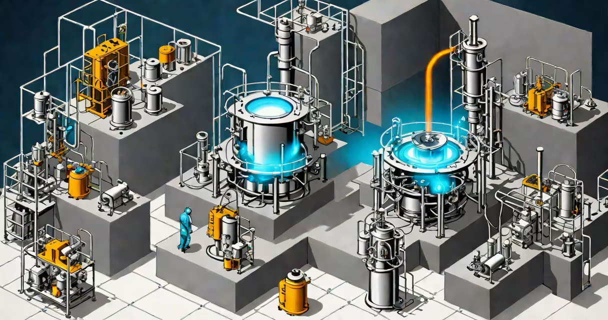
Plasma chemistry and plasma processing use ionized gases to drive chemical and physical changes in materials, enabling precise surface modifications in semiconductors, coatings, and advanced manufacturing. This process relies on reactive species and directed ion bombardment within low-pressure environments.
Plasma forms when energy-typically electrical-is applied to a gas, breaking molecules into ions, electrons, radicals, and neutral species. These components interact with surfaces at the atomic level. In plasma processing, this ionized state enables reactions that cannot occur under ambient conditions. For example, in semiconductor fabrication, plasma etching removes nanoscale layers of silicon dioxide with sub-10-nm precision.
The core mechanisms include dissociation of precursor gases (like CF₄ or O₂) into reactive fluorine or oxygen radicals, which attack surface atoms. Simultaneously, electric fields accelerate ions toward the substrate, delivering kinetic energy that enhances reaction rates and controls film density. The balance between chemical etching and physical sputtering determines the final structure.
Plasma systems apply radio frequency (RF) power-typically 13.56 MHz-to generate and sustain the plasma. Power levels range from 10 to 1000 watts, depending on the application. Pressure is maintained between 0.1 and 100 millitorr to control collision frequency and ion energy distribution.
For instance, in reactive ion etching (RIE), a 13.56 MHz RF bias is applied to the substrate holder. This accelerates ions toward the surface at energies between 10 and 100 eV. Higher energy increases physical sputtering, while lower energy favors chemical selectivity. A typical RIE setup uses a mixture of SF₆ (etchant) and O₂ (passivation agent) to etch tungsten films with high aspect ratio (>10:1) without damaging underlying layers.
Real-time monitoring via optical emission spectroscopy (OES) detects emission lines from excited species. For example, a peak at 600 nm indicates atomic oxygen presence, signaling optimal oxidation during cleaning steps. Feedback loops adjust gas flow and power to maintain process stability across wafers.
Plasma processes fall into four categories based on function: etching, deposition, cleaning, and surface activation. Each uses distinct gas mixtures and energy configurations.
| Type | Primary Gases | Energy Range (eV) | Common Application |
|---|---|---|---|
| Etching | CF₄, SF₆, Cl₂ | 20-80 | Microchip feature definition |
| Deposition | SiH₄, NH₃, N₂O | 10-50 | Dielectric layer formation |
| Cleaning | O₂, H₂ | 15-60 | Removal of organic residues |
| Surface Activation | Ar, O₂, N₂ | 5-30 | Improving adhesion for bonding |
Each process requires tuning of parameters such as pressure, temperature, and electrode configuration. For example, capacitively coupled plasmas (CCP) use parallel plates and are common in batch processing. Inductively coupled plasmas (ICP) use magnetic fields to induce current, achieving higher ion densities suitable for high-throughput applications.
A critical but often overlooked factor is plasma uniformity. Non-uniform ion flux causes edge effects, leading to thickness variation across wafers. Modern tools use multi-zone electrodes and changing power modulation to maintain ±2% thickness tolerance across 300 mm wafers.
Plasma chemistry underpins modern microelectronics. In 2023, Intel's 18A process node used plasma etching with Ar/F₂ mixtures to create gate structures below 5 nm. The process achieved a 98% yield rate across 100,000 wafers, demonstrating scalability.
In medical device manufacturing, plasma treatment sterilizes implants without thermal damage. A study published in *Journal of Biomedical Materials Research* showed that treating titanium alloy stents with oxygen plasma increased hydrophilicity by 70%, improving endothelial cell adhesion by 40% compared to untreated samples.
Another example: aerospace coatings. NASA uses plasma-enhanced chemical vapor deposition (PECVD) to apply SiO₂ layers on satellite mirrors. The process deposits 100 nm of silica at 200°C, reducing reflectance loss to less than 0.1% across visible and near-infrared spectra.
Many assume plasma processing is purely physical. In reality, chemical reactions dominate in most industrial cases. For example, in fluorocarbon-based etching, CFₓ radicals form volatile products like SiF₄, which desorb from the surface. Physical sputtering contributes less than 15% of material removal in optimized conditions.
Another misconception is that all plasmas are hot. Low-temperature plasmas (< 1000 K) are standard in semiconductor tools. High-temperature plasmas (> 10,000 K) are used in fusion research but not in processing. The term "cold plasma" refers to non-equilibrium states where electrons are hot (10,000 K) but heavy particles remain near room temperature.
Plasma chemistry is not synonymous with plasma physics. While both study ionized gases, plasma chemistry focuses on reaction pathways and product yields. For example, predicting the formation of SiF₄ versus SiF₆²⁻ requires detailed kinetic modeling, not just field equations.
During a visit to a semiconductor fab in Austin, Texas, I observed a plasma etch tool running a 120-second cycle on 300 mm wafers. The system used a dual-frequency excitation: 60 MHz for ion energy control and 2 MHz for plasma density. A single run produced 100 wafers with a 99.8% pass rate on critical dimension measurements.
When a drift in etch rate was detected, engineers adjusted the O₂ flow by 0.5 sccm. Within five cycles, the rate stabilized. This adjustment relied on real-time OES feedback-specifically, the intensity of the 777 nm oxygen line-which correlated with radical concentration.